FAQ (Frequently Asked Questions) with tutorial answers regarding the original basic patent. We have now published several reports on a revolutionary new quantum transistor that operates at room temperature. We will be preparing additional patents shortly based on the structure and the methods of fabrication of the new transistor. Our updated publications page includes short abstracts of the two most important publications, which will be published in May 2008.
You are also encouraged to ask any other questions or make suggestions by email to Don Kendall, CEO dkendall@starmega.com or Michael Kendall, President mkendall@starmega.com .
1. What does the acronym STAR stand for?
“Strongly Textured Atomic Ridges”
2. How do I see a copy of the basic patent?
A copy of the basic patent, and other StarMega patents,
can be accessed by clicking on PATENTS on the home page.
3. How would you summarize the basic patent?
It is a group of structures and methods to produce very small ridges,
islands or grooves 20 to 50 times smaller than the smallest dimensions
on a commercial integrated circuit, or IC.
One nanometer (nm) is roughly the length of 10 hydrogen atoms laid end to end.
The smallest dimension in IC production in 2008 is 45 nm (nanometers),
although several companies are already producing 22 nm dimensions in the laboratory.
Our minimum dimension of the lines is in the range of 2 nm for the line width and the center to center distance (the pitch) between the lines is about 5 nm. The crystal itself does this by using the natural crystal structure of certain perfect crystal surfaces and special processes. The lines have a Line Edge Roughness (LER)
that is much smaller than the LER of the narrowest lines and spacings
obtained with the best optical lithography. It does not depend on charged particles or light of any type, so its resolution does not have the wavelength limitations of any of the established lithographic methods. It is generally used in conjunction with standard optical lithography to make integrated circuits, field emitting display clusters, superconductors, chemically active surfaces, and other unique structures,
and of course the world’s first silicon nanowire quantum transistors that operate at room temperature.
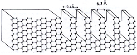
The primary difference of the structures of this patent from published work is that the extremely small original surface undulations are greatly amplified in height. This difference will be apparent in Figure 1 below comparing the ideal "natural structure" on the left side of the drawing (with about 2 Ĺ of surface topography depth) relative to the "amplified structure" on the right side of the same drawing (with etched grooves of 6.3 Ĺ width and 15 Ĺ depth on a 9.4 Ĺ pitch) after processing. The grooves can be much shallower or much deeper, depending on the application. This particular crystal orientation, the (112), allows the narrowest grooves attainable while avoiding the collapse of the groove walls.
Another important part of the patent is a novel "atomic cookie cutter" method that allows extremely regular atomic size "dots" to be produced at a much smaller scale than almost any other method. These stripe and dot surface-amplification modifications greatly expand the field of applications
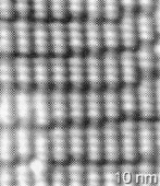
Figure 1. Natural unetched (112) cross section at left of first figure. The "Amplified morphology" is shown on the right of the figure after etching and after removal of the metal etch mask from the atomic ridges. An actual atomic resolution image of the single monolayer gallium atoms (in white) that could be used as an "etch mask" to produce the deep grooves above.
4. What is one of the patent's "unique structures"?
One of the most important structures is the Metal Oxide Semiconductor Field Effect Transistor, or MOSFET.
There are millions of these transistors in a modern IC, and the most critical part of each one is what is called the gate oxide. Great effort is usually expended to make this oxide extremely flat. However, our basic patent introduces the concept of a gate oxide with hundreds of regularly spaced small wrinkles, or undulations.
A cross-section of such a device is shown in Figure 12 of the patent application and is repeated below.
Now in a modern MOSFET, the smallest spacing between the source S and the drain D is about 450 Ĺ (45 nm). One of the favored spacings for this invention is only 16.3 Ĺ (1.63 nm) as shown in Figure 5 from the patent after producing the nanometer width grooves. These ridges are then oxidized to form an undulating insulating film and fabricated into the special MOSFET of Figure 12 from the patent. The actual number of undulations between S and D is 80 in this particular case. We should point out that in the standard device, this oxide is almost perfectly flat. On top of this oxide layer, a thin metal layer generally serves as the gate contact. It is generally flat in the standard MOSFET, and with special technology, it may also be deposited touching only the tops of the undulations (essentially flat) as in Figure 12, or it can be configured in several other ways.
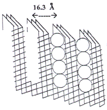
FIGURE 5. Cross section of (114) with embedded Buckyballs for superconductivity |
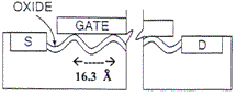
FIGURE 12. Undulating gate MOSFET |
5. How does the current behave in a standard flat-oxide MOSFET?
The current of the traditional flat-oxide device is shown as the upper dashed line below, which we have added to the patent’s Figure 14. The device often operates with "two volt logic" which means that 2 V (volts) is applied between the source and the drain, where a large dot is shown. If this voltage is placed across S and D while the gate also has a positive voltage of about two volts, it passes a current of a milliamp or so and it is said to be "on". The other operating point is with zero volts applied to the gate metal (see square dot) while the V between S and D is still 2 volts. At this point, essentially no current flows from S to D, so the device is "off". This ability of millions of transistors to switch from "one" to "zero" is the basis of the digital revolution. It allows one to count up to large numbers, to do mathematical operations at incredible speeds, and much more.
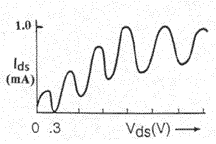
FIGURE 13. Deep groove MOSFET. |
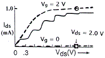
FIGURE 14. Shallow groove MOSFET. |
6. So what good are atomic size wrinkles in a MOSFET gate oxide?
The wrinkles change the device character in a major way, as shown in Figures 13 and 14 above taken from the patent. The current in the device with the regular wrinkles in the gate oxide can have a series of plateaus shown in the bottom curve of Figure 14. The reason for this is that any moving electron has a wavelength associated with it. The higher the voltage applied between the source and drain, the faster the electron travels, and the shorter the wavelength becomes. As these electrons wave along in a regular manner, they can interact with the wavy oxide in unusual ways. At certain voltages (that is, at certain electron wavelengths about the same size as the oxide undulations) the electrons move easily along the wavy oxide (see Fig. 12). At other wavelengths they slow down.
In the latter slow-down case, increasing the voltage between S and D does not increase the current (as seen in the plateaus of 14 above). In fact, the current may even decrease as the voltage increases, which leads to a "negative resistance" in certain ranges of voltage. This is shown schematically in Figure 13 from the patent. These backward slopes actually lead to some extremely interesting applications, but for integrated circuits we will focus here on the device with the plateaus of Figure 14. In particular, we are interested in the first plateau between 0.2 and 0.3 Volts. You will notice that the general shape of the first plateau looks almost exactly the same as the upper curve in Figure 14 for the standard MOSFET, but now the current and voltage are both much smaller where the plateau occurs. This suggests that the same logic operations might be performed at perhaps 10 times lower voltage and current. This is a very important result.
7. What is the advantage of a 10 times lower operation voltage?
The power dissipation may be as much as 100 times smaller than the standard MOSFET! This follows from the ten times lower voltage and from the freshman physics formula for power P, which is: P = V2/R , where R depends on a number of parameters in an IC and must be defined as an "effective resistance". If this much lower power consumption of a MOSFET can be extended to the same margin of advantage in a complex IC, then your laptop computer might operate 200 hours without charging the batteries instead of going dead after two hours. Furthermore, your cell phone might stay active for months without charging. Again, an important result.
Finally, the speed of operation may be as much as 10 times faster, since it takes much less time to apply (and remove) 0.2 V than it does 2.0 V. To obtain this speed advantage, the current on the plateau may need to be increased by a changing the device geometry or making other changes. This will increase the power consumption somewhat, but it will still be much lower than a standard "flat oxide" MOSFET.
8. Do the electrons move faster in these structures?
This is a complex question for the electrons flowing perpendicular to the undulations of Figure 12 above, since quantum tunneling from ridge to ridge is involved. Also, MOSFET structures with widths in the 10 to 50Ĺ range have not yet been fabricated, though wider multi-finger (~500Ĺ) structures suggest that the mobility is still well behaved for perpendicular current.
However, the carrier mobility (of electrons or holes) may indeed be greatly enhanced when the source and drain are oriented so that the carriers move parallel to the ridges, that is, into the page of Figure 12. This is because these parallel carriers in the inversion layer stripes do not scatter sidewise or backwards nearly as often as they would in the sheet of electrons under the flat oxide. A higher mobility, of course, allows the carriers to pass from source to drain much faster, and thereby increases the operation speed of the IC.
9. Are the resulting structures easily detectable in the finished devices?
Yes. The change in the electrical character will be quite evident, and the atomic wrinkles can also be easily detected using either AFM (atomic force microscope), or with a bit more difficulty with cross-sectional STEM (scanning transmission electron microscopy). This easy detectability is important to enforcing a patent.
10. What is the most challenging aspect of this radical new technology?
At this moment, it appears that the biggest challenge will be to produce significant portions of a (5 5 12) or other (1 1 X) wafer that are perfectly atomically flat. This difficulty is due to the fact that a particular crystal orientation of a wafer is rarely more precise than about 0.1°, and it needs to be precise to 0.01ş to have even a 1µm wide atomically flat region. Even more serious is the fact that even the best-aligned chem-mechanical polishing (CMP) process produces only small regions of atomic flatness, randomly scattered around the surface of the wafer.
The basic patent addresses this problem with a technology that
forces the atomically flat regions to appear in the precise locations
where the critical regions of the manufactured devices are to be placed.
There are several variants of this general concept covered in the Baski-Kendall 2002 patent.
The important point is that it can be done in a production process. This certainly has relevance in the IC applications, but also in the micro-tip-array application of the Field Emitting Device (FED), as well as in superconductor, chemical, biological, light emitter and IR lasers, and other applications not discussed here.
11. How would this technology be demonstrated on some shorter range applications?
The most direct demonstration was to make and test some MOSFETs in the two major current directions, both parallel and perpendicular to the atomic stripes. This was done without any complex etching steps on (5 5 12), (114) and (100) wafers handled in exactly the same manner within the same processing run using standard fabrication methods on these abnormal crystal surfaces. We did this.in a Mexican National Laboratory that Dr. Kendall helped establish between 1975 and 1984 after a 17 year career in research at Texas Instruments in Dallas.
The results are discussed in the papers found on the publications page.
You may find that the one dimensional artificial atoms that we discovered are the most interesting.
Just imagine what an artificial atom would look like if a few electrons
were squeezed into an incredibly small needle that was just a few atoms wide
instead of into a very small sphere like in a real atom. The artificial atom is indeed very interesting, but we are presently focused on more practical applications.